Reliable PCB Manufacturing Services
Delivering precision-engineered PCB solutions with fast turnaround, consistent quality, and advanced manufacturing technology.
From prototype to production, we provide end-to-end PCB manufacturing services tailored to meet the demands of modern electronics industries.
Your Trusted PCB Manufacturing Partner
Delivering Precision PCB Solutions
With cutting-edge manufacturing and a commitment to quality, we provide PCB services that power innovation across industries.
We Provide Best Service
We provide complete PCB solutions including PCB design, PCB manufacturing, and PCB assembly. With advanced technology, high precision, and strict quality control, we deliver reliable PCBs with fast turnaround time. Our focus on quality, efficiency, and customer satisfaction makes us your trusted PCB partner.

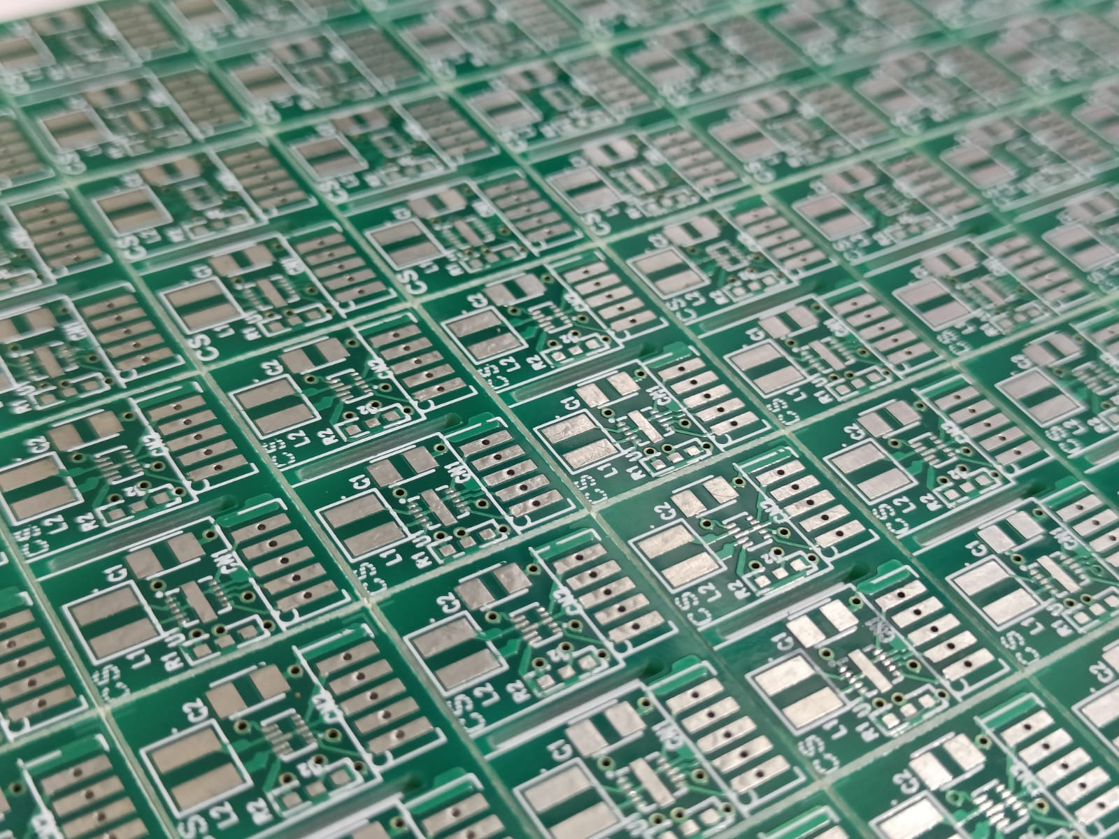
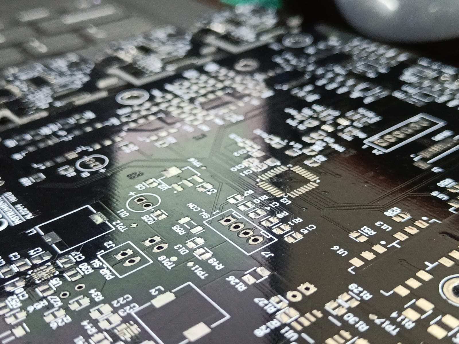
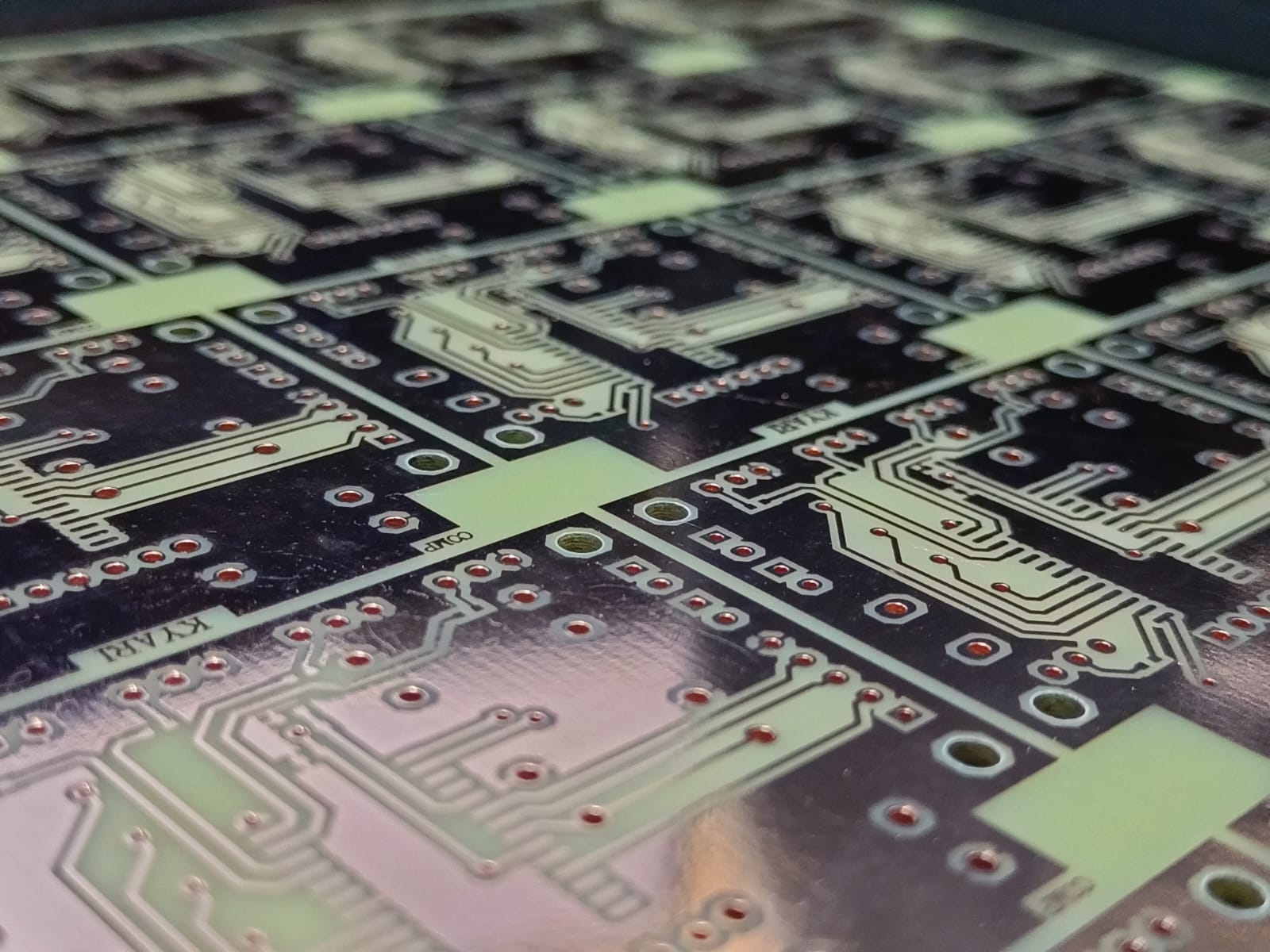
PCB Manufacturing
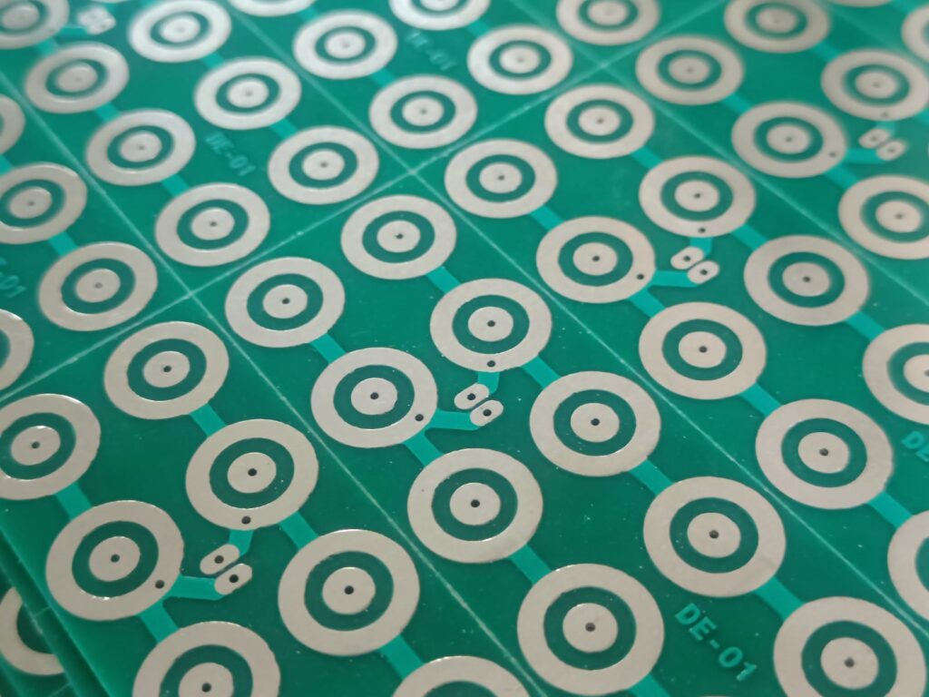
We produce high-quality single-sided, double-sided, and metal core PCBs using advanced machinery and strict quality standards. Our process ensures durability, accuracy, and consistent performance.

PCB Design
Our expert team provides custom PCB design solutions, optimized for performance and manufacturability. We support schematic design, layout, and design verification to ensure flawless results.

PCB Assembly
We offer reliable PCB assembly services with precision component placement and quality inspection. From prototype to bulk production, we ensure efficient and defect-free assembly.
Quality You Can Trust
Our Complete PCB Production Process
From Sales inquiry to final dispatch, our streamlined process ensures precision, quality, and timely delivery at every stage of PCB production.
1. Sales & Marketing Department
Sales & Marketing Department
The Sales & Marketing team works closely with customers to understand their PCB requirements.
They gather technical details, specifications, and project expectations. Based on the requirement, they process and confirm the order for production.
2. Design & Engineering
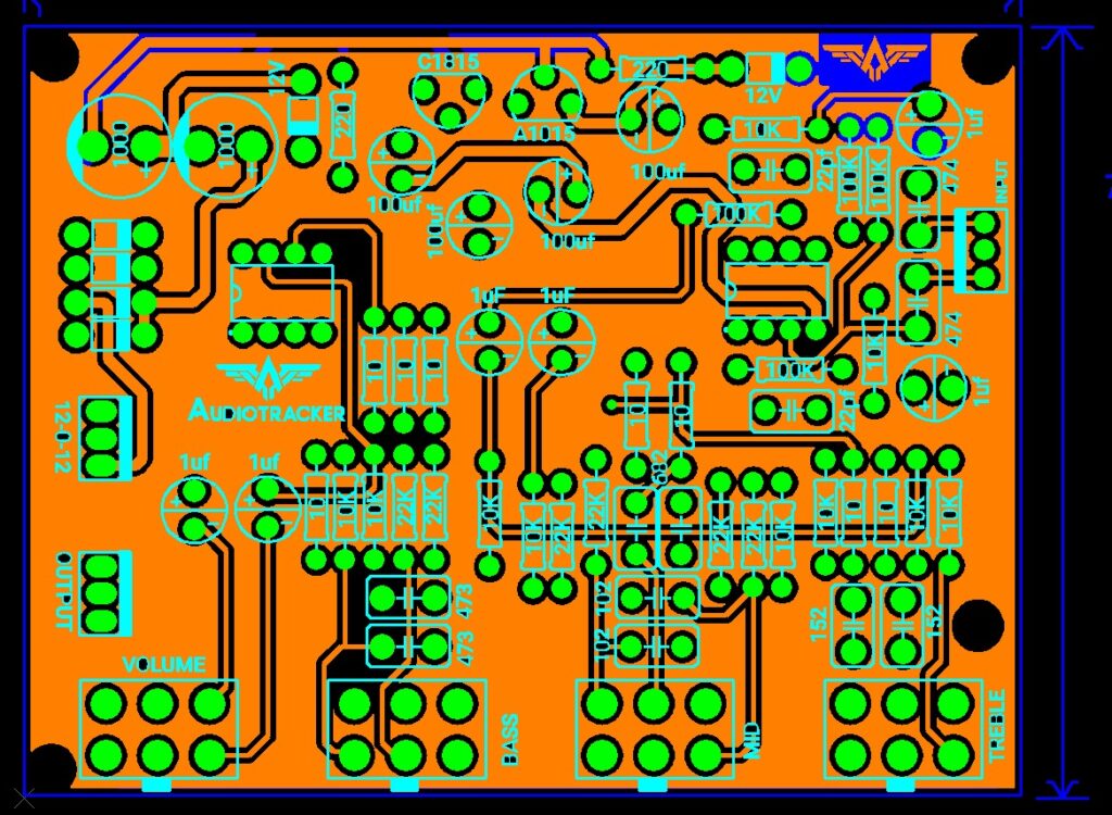
Design & Engineering (CAD-CAM)
Engineering is a critical process in PCB manufacturing. Our engineering team works closely with production throughout the product lifecycle.
We handle complex designs while aligning with technical specifications and plant capabilities.
This ensures cost-effective, efficient, and high-quality PCB production.
3. Sheet Cutting Department
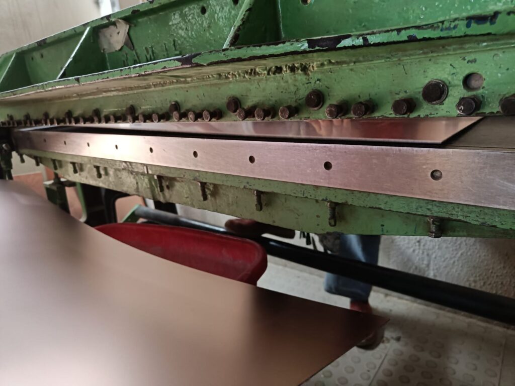
Sheet Cutting Department
The shearing department has different material storage and cutting the exact size of launch pcbs as per panel or quantity. The laminate sheet of material for different material as per job card launch after by engineering department.
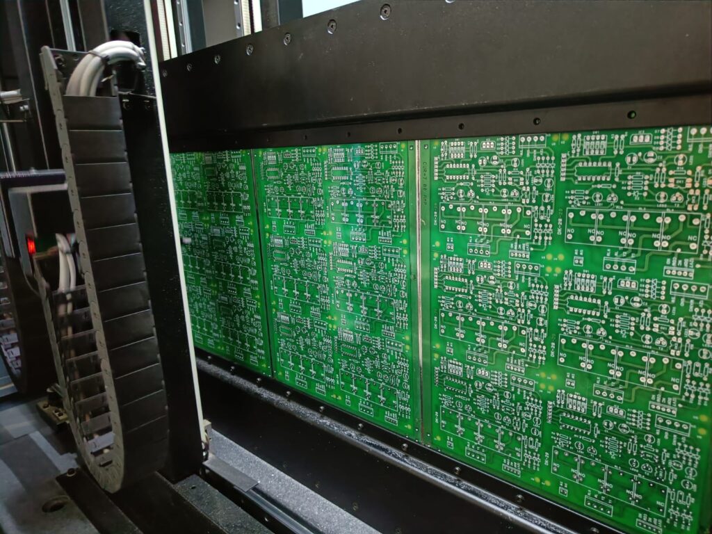
4. CNC Drilling Department
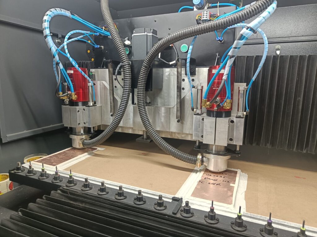
CNC Drilling Department
Holes are drilled using CNC machines to create vias and component mounting points.
This process ensures accurate top-to-bottom electrical connections. Excess copper is removed to prepare the PCB for further processing.
5. PTH (Plated Through Hole) Process
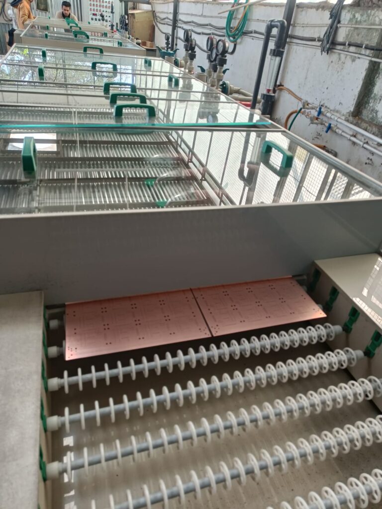
PTH (Plated Through Hole) Process
Drilled holes are chemically cleaned and activated for plating. Copper is deposited inside the holes to create electrical connections between layers.
This process ensures strong conductivity and reliable PCB performance.
6. Image Processing(Track Printing)
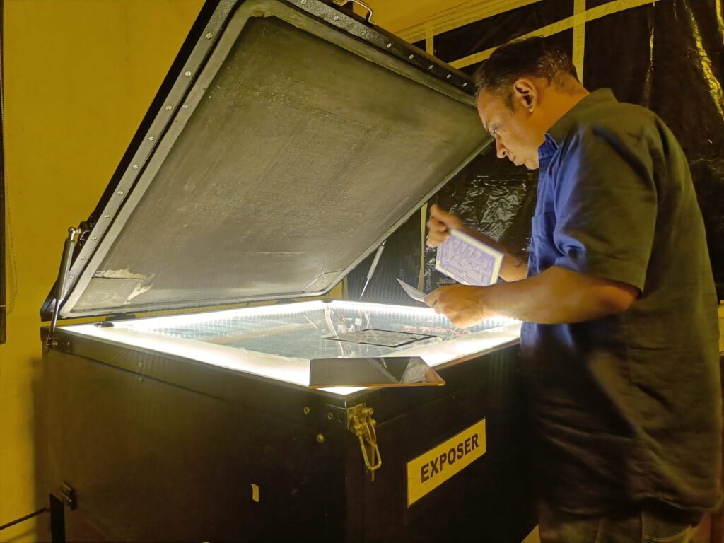
Image Processing(Track Printing)
PCB layout is transferred using UV exposure technology. Circuit patterns are accurately printed on the board. Ensures clear and precise design formation.
7. Plating (Electroplating)
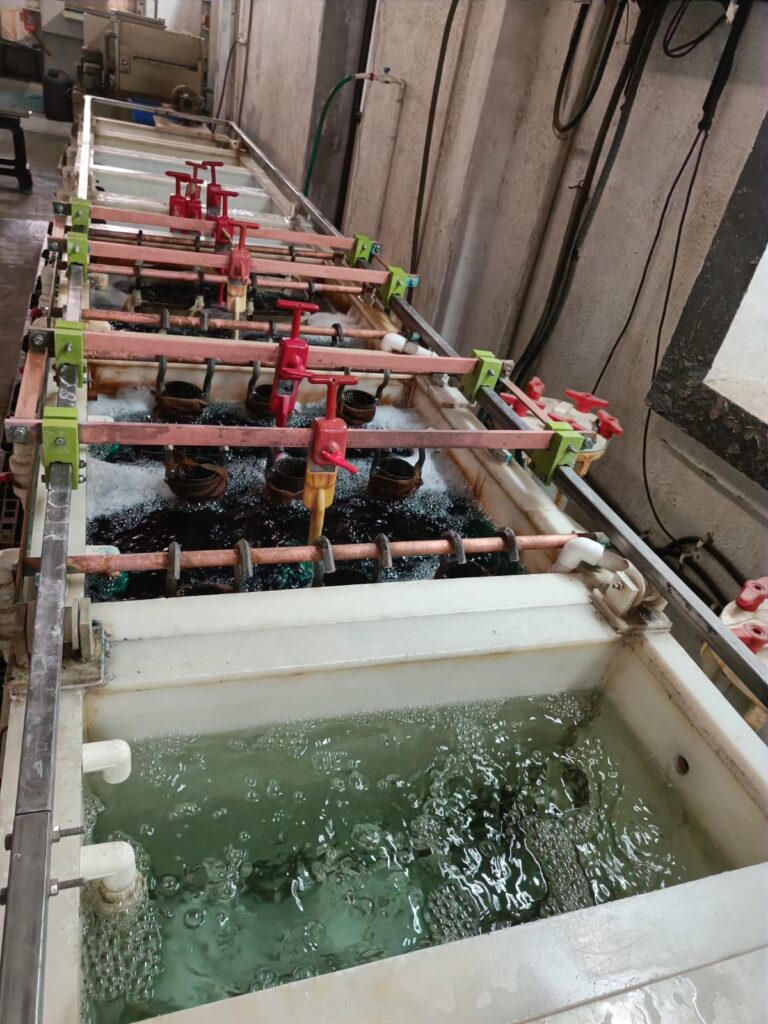
Plating (Electroplating)
Copper is deposited on holes and PCB surface.
Ensures strong electrical connections between layers. Improves conductivity and durability.
8. Etching Process
Etching Process
Unwanted copper is removed chemically from the board. Only required circuit paths remain intact.
Creates the final conductive pattern.
9. Solder Mask
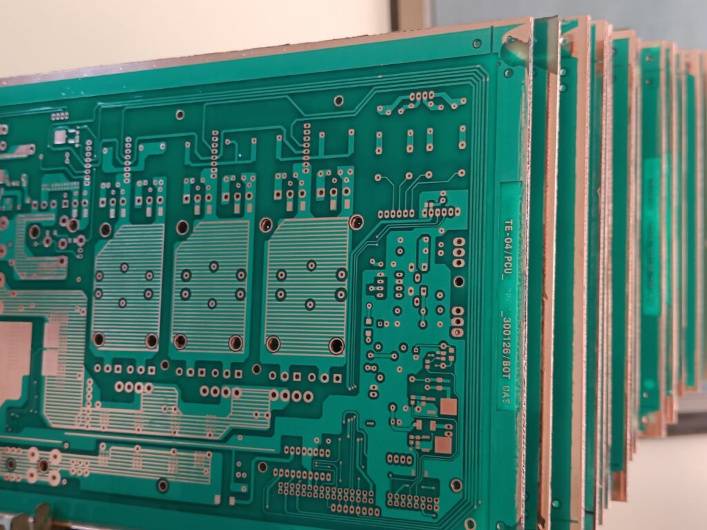
Solder Mask
A protective layer is applied over the PCB surface.
Prevents oxidation and short circuits.
Enhances board reliability.
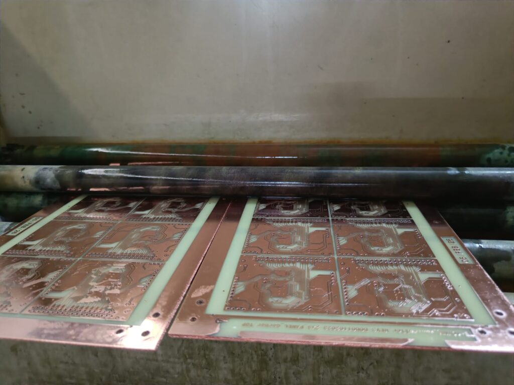
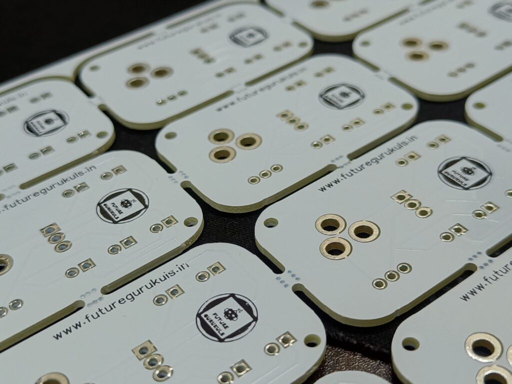
10. Surface Finishing
Surface Finishing
Finishing like HASL is applied for solderability.
Protects copper from environmental damage.
Ensures smooth assembly process.
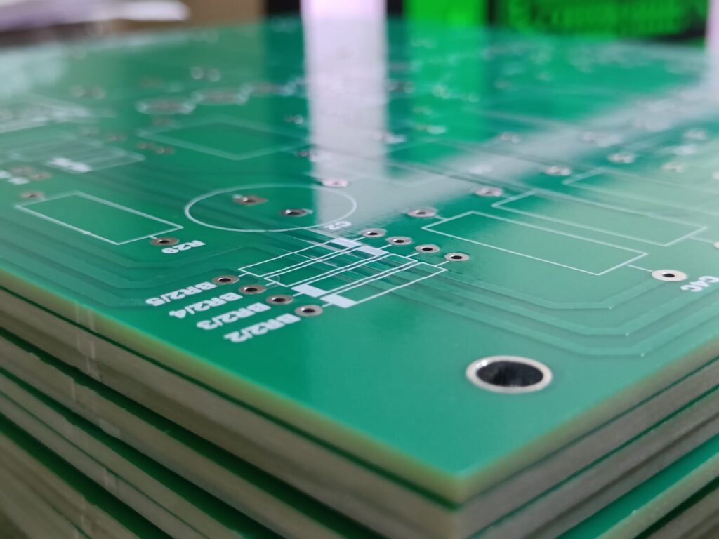
11. Silkscreen Printing
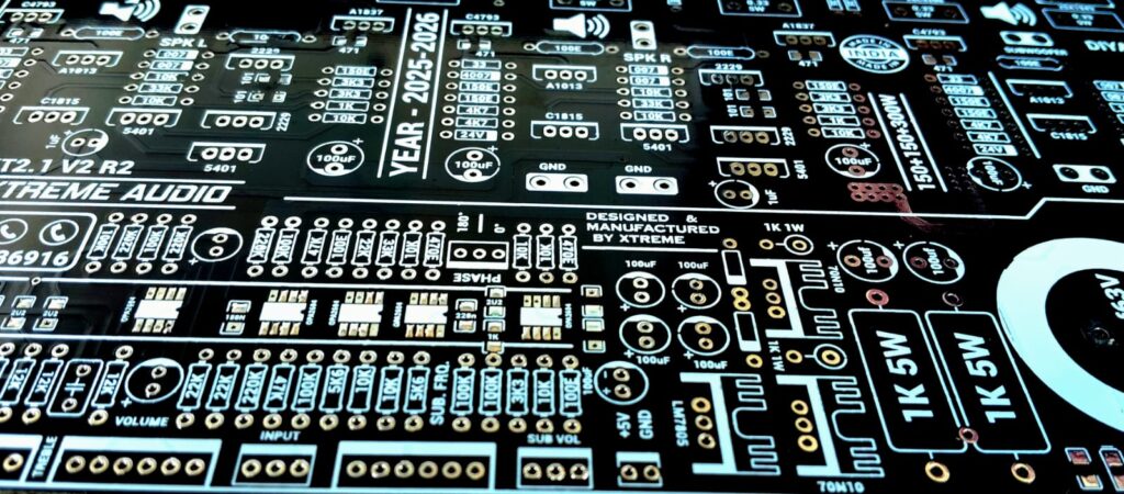
Silkscreen Printing
Component details and labels are printed on PCB.
Helps in easy identification during assembly.
Improves usability and clarity.
13. Testing & Inspection
Testing & Inspection
Each PCB is tested for electrical performance.
Quality checks ensure zero defects.
Meets industry standards and reliability.
14. Routing & Profiling
Routing & Profiling
PCB is cut into final shape and size.
Done using routing or V-cut machines.
Ensures precise dimensions.
15. Final Dispatch
Final Dispatch
Final inspection is performed before packaging.
Boards are packed safely for delivery.
Ensures timely and secure shipment.